- 您现在的位置:买卖IC网 > Sheet目录3887 > PIC16F872T-E/SO (Microchip Technology)IC MCU CMOS 20MHZ 2K FLSH 28SOIC
141
8048C–AVR–02/12
ATtiny43U
19. Memory Programming
This section describes the different methods for Programming the ATtiny43U memories.
19.1
Program And Data Memory Lock Bits
The ATtiny43U provides two Lock bits which can be left unprogrammed (“1”) or can be pro-
grammed (“0”) to obtain the additional security listed in Table 19-2 on page 141. The Lock bits
can only be erased to “1” with the Chip Erase command.
The device has no separate boot loader section. The SPM instruction is enabled for the whole
Flash, if the SELFPROGEN fuse is programmed (“0”), otherwise it is disabled.
Program memory can be read out via the debugWIRE interface when the DWEN fuse is pro-
grammed, even if lock bits are set. Thus, when lock bit security is required, debugWIRE should
always be disabled by clearing the DWEN fuse.
Note:
1. “1” means unprogrammed, “0” means programmed
Notes:
1. Program fuse bits before programming LB1 and LB2.
2. “1” means unprogrammed, “0” means programmed
Lock bits can also be read by device firmware. See section “Reading the Fuse and Lock Bits
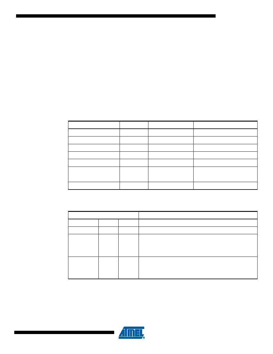
Table 19-1.
Lock Bit Byte
Lock Bit Byte
Bit No
Description
Default Value
7
–
1 (unprogrammed)
6
–
1 (unprogrammed)
5
–
1 (unprogrammed)
4
–
1 (unprogrammed)
3
–
1 (unprogrammed)
2
–
1 (unprogrammed)
LB2
1
Lock bit
1 (unprogrammed)
LB1
0
Lock bit
1 (unprogrammed)
Table 19-2.
Lock Bit Protection Modes.
Memory Lock Bits
Protection Type
LB Mode
LB2
LB1
1
No memory lock features enabled.
21
0
Further programming of the Flash and EEPROM is disabled in
High-voltage and Serial Programming mode. The Fuse bits are
locked in both Serial and High-voltage Programming mode.
debugWire is disabled.
30
0
Further programming and verification of the Flash and EEPROM
is disabled in High-voltage and Serial Programming mode. The
Fuse bits are locked in both Serial and High-voltage
Programming mode.
(1) debugWire is disabled.
发布紧急采购,3分钟左右您将得到回复。
相关PDF资料
PIC16F727-E/P
IC PIC MCU FLASH 8KX14 40-DIP
PIC16F871T-E/PT
IC MCU CMOS 20MHZ 2K FLSH 44TQFP
PIC16F871T-E/L
IC MCU CMOS 20MHZ 2K FLSH 44PLCC
PIC16F871-E/PT
IC MCU CMOS 20MHZ 2K FLSH 44TQFP
PIC16F871-E/L
IC MCU CMOS 20MHZ 2K FLSH 44PLCC
PIC16F870T-E/SS
IC MCU CMOS 20MHZ 2K FLSH 28SSOP
PIC16F870T-E/SO
IC MCU CMOS 20MHZ 2K FLSH 28SOIC
PIC16F84AT-20E/SS
IC MCU CMOS 20MHZ 1K FLSH 20SSOP
相关代理商/技术参数
PIC16F872T-E/SS
功能描述:8位微控制器 -MCU 3.5KB 128 RAM 22 I/O RoHS:否 制造商:Silicon Labs 核心:8051 处理器系列:C8051F39x 数据总线宽度:8 bit 最大时钟频率:50 MHz 程序存储器大小:16 KB 数据 RAM 大小:1 KB 片上 ADC:Yes 工作电源电压:1.8 V to 3.6 V 工作温度范围:- 40 C to + 105 C 封装 / 箱体:QFN-20 安装风格:SMD/SMT
PIC16F872T-I/SO
功能描述:8位微控制器 -MCU 3.5KB 128 RAM 22 I/O RoHS:否 制造商:Silicon Labs 核心:8051 处理器系列:C8051F39x 数据总线宽度:8 bit 最大时钟频率:50 MHz 程序存储器大小:16 KB 数据 RAM 大小:1 KB 片上 ADC:Yes 工作电源电压:1.8 V to 3.6 V 工作温度范围:- 40 C to + 105 C 封装 / 箱体:QFN-20 安装风格:SMD/SMT
PIC16F872T-I/SS
功能描述:8位微控制器 -MCU 3.5KB 128 RAM 22 I/O RoHS:否 制造商:Silicon Labs 核心:8051 处理器系列:C8051F39x 数据总线宽度:8 bit 最大时钟频率:50 MHz 程序存储器大小:16 KB 数据 RAM 大小:1 KB 片上 ADC:Yes 工作电源电压:1.8 V to 3.6 V 工作温度范围:- 40 C to + 105 C 封装 / 箱体:QFN-20 安装风格:SMD/SMT
PIC16F872T-I/SS033
制造商:Microchip Technology Inc 功能描述:
PIC16F873-04/SO
功能描述:8位微控制器 -MCU 7KB 192 RAM 22 I/O RoHS:否 制造商:Silicon Labs 核心:8051 处理器系列:C8051F39x 数据总线宽度:8 bit 最大时钟频率:50 MHz 程序存储器大小:16 KB 数据 RAM 大小:1 KB 片上 ADC:Yes 工作电源电压:1.8 V to 3.6 V 工作温度范围:- 40 C to + 105 C 封装 / 箱体:QFN-20 安装风格:SMD/SMT
PIC16F873-04/SO
制造商:Microchip Technology Inc 功能描述:8BIT FLASH MCU SMD 16F873 SOIC28
PIC16F873-04/SP
功能描述:8位微控制器 -MCU 7KB 192 RAM 22 I/O RoHS:否 制造商:Silicon Labs 核心:8051 处理器系列:C8051F39x 数据总线宽度:8 bit 最大时钟频率:50 MHz 程序存储器大小:16 KB 数据 RAM 大小:1 KB 片上 ADC:Yes 工作电源电压:1.8 V to 3.6 V 工作温度范围:- 40 C to + 105 C 封装 / 箱体:QFN-20 安装风格:SMD/SMT
PIC16F873-04/SP
制造商:Microchip Technology Inc 功能描述:IC 8BIT FLASH MCU 16F873 SDIL28